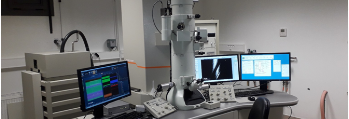
TEM JEOL 2100
Microscope manager
Nicholas Blanchard (ILM)
Presentation of the microscope
This "workhorse" TEM is ideally suited for conventional transmission electron microscopy. E.g. Studying extended defects/dislocations, size and shape of nano-objects (nanoparticles, nanotubes and nanowires) and electron diffraction.
Microscope features
The JEOL 2100 is equipped with a high tilt pole piece with a point-to-point resolution of 0.25 nm at 200 kV. The minimum probe size is ~1 nm. The microscope is equipped with a STEM module and both a bright field and annular dark field detector.
The microscope is aligned at 80, 120 & 200 kV and is equipped with a bottom mount Orius SC1000 CCD camera (Gatan)
Analytical accessories
EDX XMAX 80mm² & Aztec software (OXFORD INSTRUMENTS)
Sample holders
JEOL single tilt holder (X-tilt: +/-42°), JEOL analytical Be double-tilt holder (X-tilt: +/-42°, Y-tilt)
Photograph library
 |
| Bright field TEM image of a SiC nanowire |
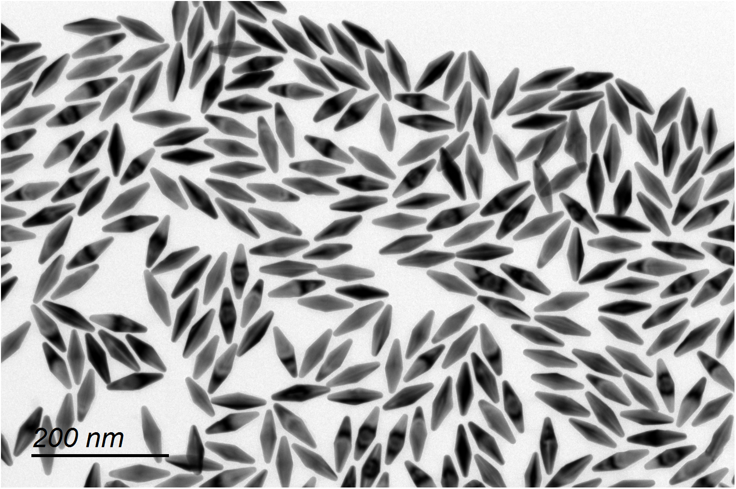 |
| Bright field TEM image of bipyramid Au nanoparticles |
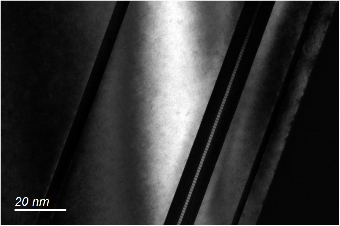 |
| Two beam (g = 002) dark field TEM image of a MBE grown layered structure: InP/AlAs/InAlAs/ InGaAs |
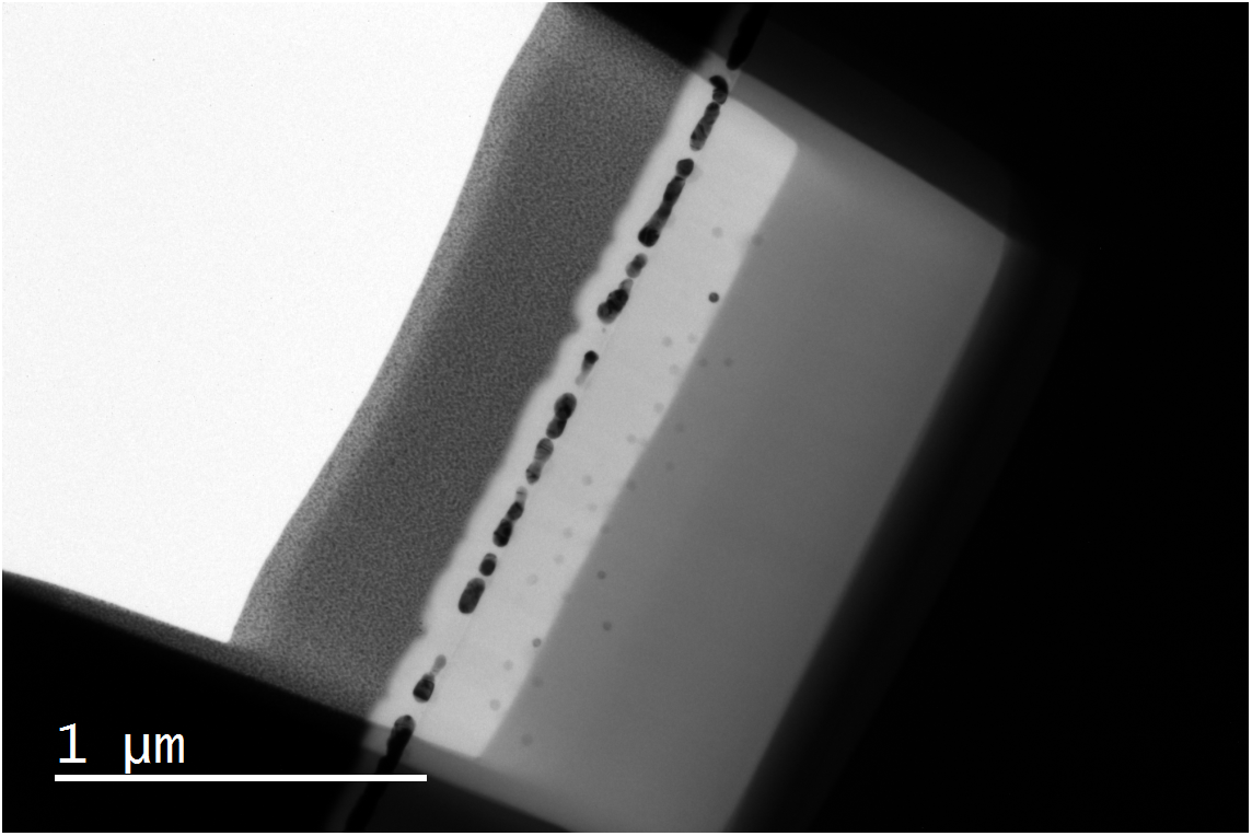 |
| Bright field TEM image of thin foil prepared by FIB |
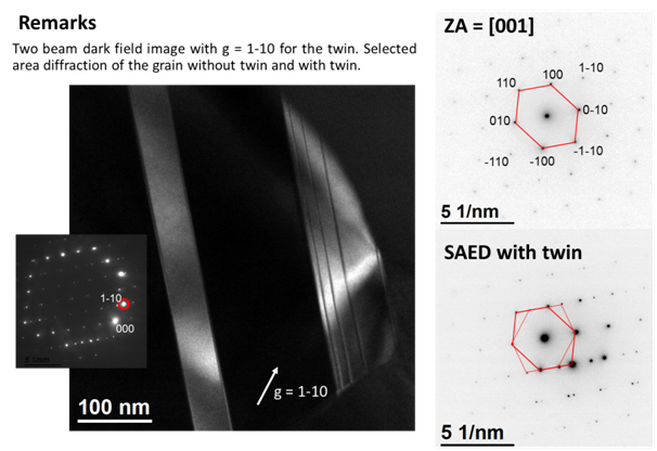 |
| Two beam (g = 1-10) dark field TEM image of twin defects in a single grain in a boron carbide ceramic |
