TEM JEOL 2010F
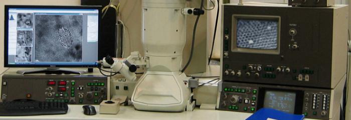
Microscope team
Clémentine Fellah (LGL-TPE, ENS Lyon), Laurence Burel (ICELYON, CNRS), Lucian Roiban (Mateis, INSA de Lyon).
Presentation of the microscope
The JEOL 2010F microscope, installed in CLYM, is a field-emission transmission electron microscope, with a resolution of 0.195 nm and a minimum probe size of 0.3 nm (0.5 nm, standard conditions). This TEM operates at 200kV and uses a Schottky field emitter. These characteristics make it a high-resolution and high-performance instrument for the characterization of a wide range of samples. A STEM device allows the acquisition of images in High Angle Annular Dark Field (HAADF).
Microscope features
The JEOL 2010F microscope is equipped with several analytical systems:
- An EDX X MAX 80 system (OXFORD INSTRUMENTS),
- A DigiPEELS system (GATAN) with an optimal energy resolution of 0.65 eV (1-1.2 eV, standard conditions).
JEOL single-tilt and double-tilt sample holders are available as well as a tip for single-tilt tomography (+/- 85°).
Photograph library
High-resolution instrument
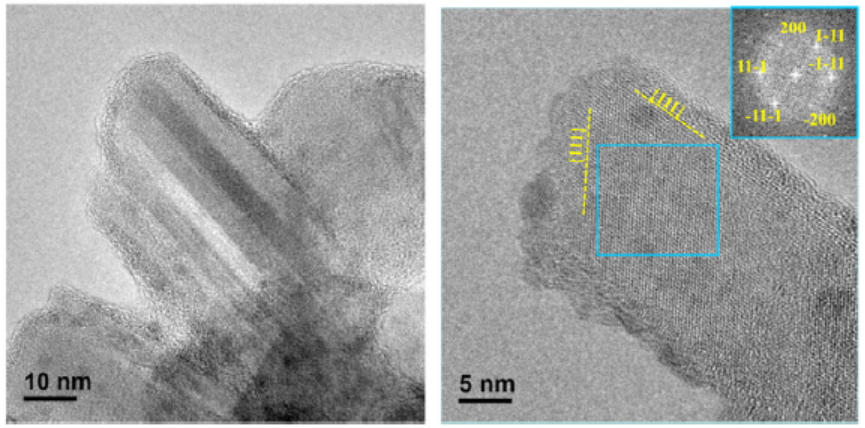 |
Nanoporous silicon powder (NP-Si) TEM (left) and HRTEM (right) images with FT calculated inside the blue square. |
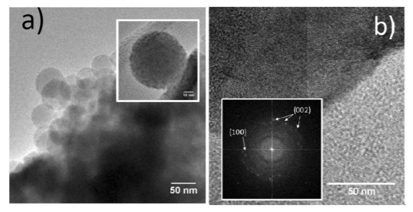 |
TEM (a.) and HRTEM (b.) images with FT of ZnO-PAA nano-hybride with 0.1% Mn |
STEM
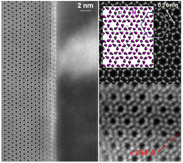 |
Yttrium oxide doped Si3N4 polycrystal : grain boundary and detail of the resolution of the HAADF silicon subnetwork. |
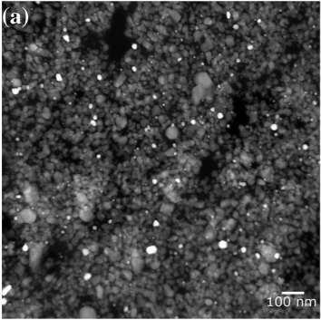 |
STEM HAADF observation of a Ag :TiO2 film |
EDX XMAX 80 system
 |
|
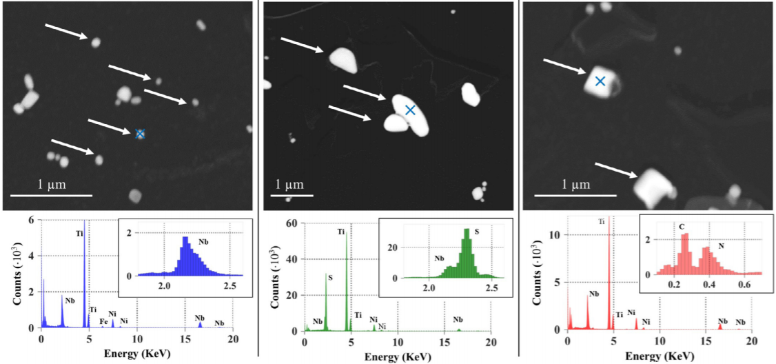
STEM-HAADF observation of three populations of precipitates (a : (Ti,Nb)C, b : Ti4C2S2, c : TiN) found in steel with associated EDX spectra. |
DigiPEELS system
 |
|
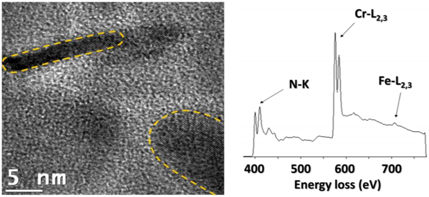
HRTEM image of nitride replicas on carbon film (left) and associated electron energy loss spectroscopy spectrum (EELS) that indicates iron in these chromium-rich nitrides (right) doi : 10.3390/ma11081409 |
